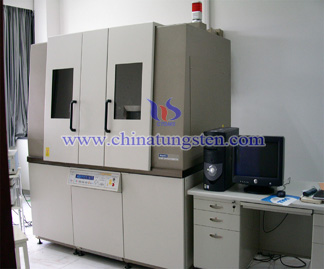
Blue Tungsten Oxide Testing Equipment

Blue tungsten oxide testing equipment according to different testing methods includes x-ray diffraction, scanning electron microscopy, photoelectron spectroscopy, electron energy analyzer, transmission electron microscopy. X-ray diffraction is using x-ray to study the inner microstructure of material, widely used in major universities, research institutes and factories and mines. Its basic structure includes high stability X-ray source, sample and sample position orientation adjustment mechanism system, ray detector and diffraction pattern processing analysis system. SEM was invented in 1965 to study modern cytobiology, mainly use secondary electron signal imaging to observe the surface morphology of the sample which is using narrow electron beam to scan the sample by electron beam interaction with the sample, it is mainly about secondary electron emission.
The photoelectron spectrometer consists of six parts: excitation source, sample ionization chamber, electronic energy analyzer, electronic detector, vacuum system and data processing system. The source of ultraviolet radiation and X-ray source are commonly used. The use of ultraviolet radiation source as the excitation source called ultraviolet photoelectron spectroscopy, the use of X-ray known as X-ray photoelectron spectroscopy, collectively referred to as photoelectron spectroscopy.
Electron energy analyzer: the role is to measure the energy distribution emitted from the surface of sample, the photoelectron spectrum is a flow of electrons relative to the kinetic energy of the map.
Transmission Electron Microscope (TEM), microstructure can not be seen in the optical microscope is clear under TEM. These structures are called sub-microstructure or ultrastructure. To see these structures, you must choose a shorter wavelength light source to improve the resolution of the microscope. In 1932, Ruska invented the electron beam as the light source of the transmission electron microscope, the electron beam wavelength is much shorter than visible light and ultraviolet light, and the wavelength of the electron beam and the electron beam emitted voltage is inversely proportional to the square root, that the higher the voltage, the shorter the wavelength. At present the resolution of TEM can reach 0.2nm.


